
Daksh C.
PCB Design Engineer | Hardware Layout & DFM Optimization Expert
 Jalandhar,
India
Jalandhar,
India
Global rank:
5,230
/
149,850
Skill pts: 11
About
Industrial-Grade PCB Layout, Hardware Prototyping & DFM Optimization Services
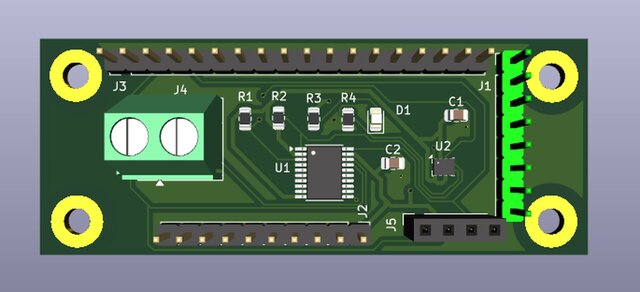
I provide full-cycle electronics engineering, schematic translation, and manufacturing-optimized PCB layout services. Utilizing industry-standard design disciplines (with native proficiency in KiCad), I specialize in transforming conceptual circuit designs into stable, high-performance physical hardware. My expertise spans custom microcontroller expansion shields (Arduino Mega/ESP32 formats), multi-channel sensor integration arrays, bi-directional logic level-shifting networks, and localized decoupling architectures.
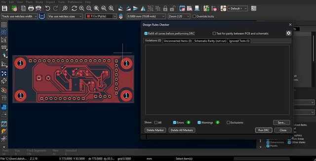
My design methodology prioritizes advanced Design for Manufacturing (DFM) principles to completely mitigate automated SMT assembly risks—such as component tombstoning—by implementing symmetrical center-trace entries on passives. Furthermore, my layouts emphasize signal integrity through unbroken ground return plane topologies to drastically minimize loop inductance and eliminate electromagnetic interference (EMI). Every project undergoes a meticulous Design Rules Check (DRC) to ensure a 100% zero-defect rate before final handoff.
... more »
« less
I provide full-cycle electronics engineering, schematic translation, and manufacturing-optimized PCB layout services. Utilizing industry-standard design disciplines (with native proficiency in KiCad), I specialize in transforming conceptual circuit designs into stable, high-performance physical hardware. My expertise spans custom microcontroller expansion shields (Arduino Mega/ESP32 formats), multi-channel sensor integration arrays, bi-directional logic level-shifting networks, and localized decoupling architectures.
My design methodology prioritizes advanced Design for Manufacturing (DFM) principles to completely mitigate automated SMT assembly risks—such as component tombstoning—by implementing symmetrical center-trace entries on passives. Furthermore, my layouts emphasize signal integrity through unbroken ground return plane topologies to drastically minimize loop inductance and eliminate electromagnetic interference (EMI). Every project undergoes a meticulous Design Rules Check (DRC) to ensure a 100% zero-defect rate before final handoff.
Portfolio
Service offers
Experience
- Freelance PCB Design & Hardware Engineer Freelance / Self-employed · Freelance Jul 2026 – Present 3 mos Ghaziabad, UP, India
Education
- Harcourt butler technical university B . E, ELECRICAL ENGINEERING, 8 2025 – 2029 (expected) Activities and Societies: IEEE NSS Robotics Society Focused on core engineering principles including electronic circuit design, microcontrollers, and digital system design. Acquired practical, hands-on experience in schematic capture, PCB prototyping, and hardware testing through academic labs and independent projects. Developed a strong foundation in analyzing signal integrity and implementing industry-standard design rules.
Other experience
- Hardware Prototyping & DFM Auditing Actively perform Design for Manufacturing (DFM) reviews on electronics prototypes to eliminate production issues such as component tombstoning, signal integrity loop delays, and acute-angle acid traps. Experienced in utilizing 3D CAD modeling software to run structural audits on board design components before factory fabrication.
Licenses & Certifications
- KiCad Direct-to-Manufacturing Mastery Course Jul 2026 – Present
- Advanced PCB Layout and Signal Integrity Design Jul 2026 – Present
Stats
0 followers, 0 following
Age: 20
Joined: July 9, 2026
Last seen: October 6, 2026
Area of Expertise
Languages
English Professional working proficiency
Hindi Native or bilingual proficiency
Punjabi (Eastern) Professional working proficiency
Location
Jalandhar, India