I offer custom PCB design and hardware layout engineering services



About this service
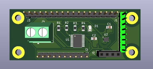
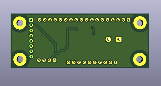
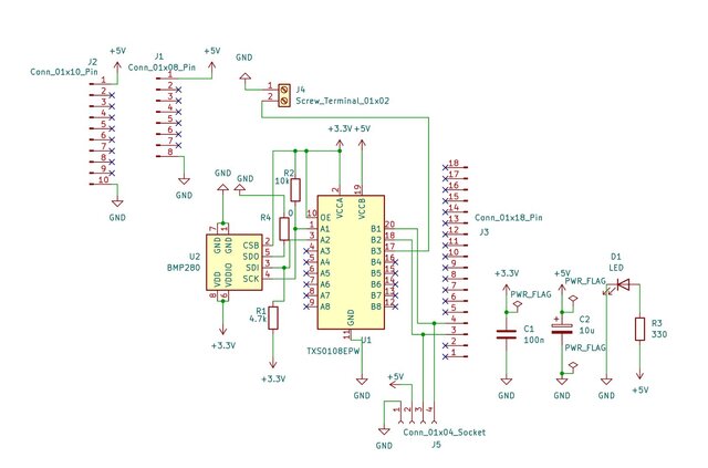
I offer professional, production-ready 2-layer and multi-layer custom PCB design and expansion shield layout services using KiCad. My engineering process turns schematic concepts into stable physical hardware optimized for industrial-grade data acquisition and high reliability. The final deliverables feature unbroken copper ground planes to minimize electromagnetic interference and ensure direct, low-inductance return paths for all signal traces.
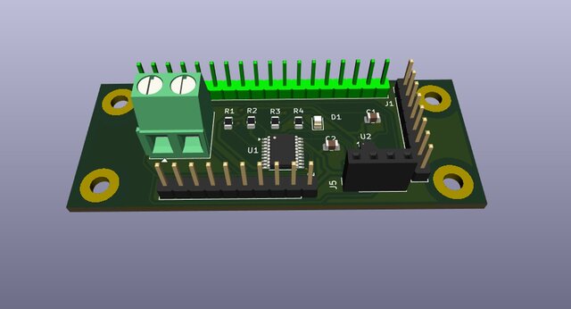
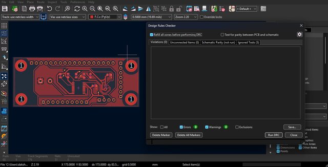
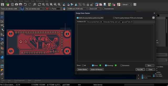
To guarantee flawless manufacturing and eliminate assembly issues like component tombstoning, all surface-mount device pad trace entries are meticulously optimized to exit centered and perpendicular to the component edges. Every layout undergoes a strict Design Rules Check with zero errors and zero unconnected lines before delivery. Additionally, all silkscreen component labels are verified using 3D visual analysis to ensure perfect legibility after assembly.
My complete engineering handoff package includes universal production Gerber files (copper, mask, stencil paste, and edge layers), precise numerical control drill files compatible with any fabrication house, high-resolution ray-traced 3D visual renders for documentation, a structured Bill of Materials mapping component packages, and full ownership of the native editable source files.
To guarantee flawless manufacturing and eliminate assembly issues like component tombstoning, all surface-mount device pad trace entries are meticulously optimized to exit centered and perpendicular to the component edges. Every layout undergoes a strict Design Rules Check with zero errors and zero unconnected lines before delivery. Additionally, all silkscreen component labels are verified using 3D visual analysis to ensure perfect legibility after assembly.
My complete engineering handoff package includes universal production Gerber files (copper, mask, stencil paste, and edge layers), precise numerical control drill files compatible with any fabrication house, high-resolution ray-traced 3D visual renders for documentation, a structured Bill of Materials mapping component packages, and full ownership of the native editable source files.
I offer professional, production-ready 2-layer and multi-layer custom PCB design and expansion shield layout services using KiCad. My engineering process turns schematic concepts into stable physical hardware optimized for industrial-grade data acquisition and high reliability. The final deliverables feature unbroken copper ground planes to minimize electromagnetic interference and ensure direct, low-inductance return paths for all signal traces.
To guarantee flawless manufacturing and eliminate assembly issues like component tombstoning, all surface-mount device pad trace entries are meticulously optimized to exit centered and perpendicular to the component edges. Every layout undergoes a strict Design Rules Check with zero errors and zero unconnected lines before delivery. Additionally, all silkscreen component labels are verified using 3D visual analysis to ensure perfect legibility after assembly.
My complete engineering handoff package includes universal production Gerber files (copper, mask, stencil paste, and edge layers), precise numerical control drill files compatible with any fabrication house, high-resolution ray-traced 3D visual renders for documentation, a structured Bill of Materials mapping component packages, and full ownership of the native editable source files.
To guarantee flawless manufacturing and eliminate assembly issues like component tombstoning, all surface-mount device pad trace entries are meticulously optimized to exit centered and perpendicular to the component edges. Every layout undergoes a strict Design Rules Check with zero errors and zero unconnected lines before delivery. Additionally, all silkscreen component labels are verified using 3D visual analysis to ensure perfect legibility after assembly.
My complete engineering handoff package includes universal production Gerber files (copper, mask, stencil paste, and edge layers), precise numerical control drill files compatible with any fabrication house, high-resolution ray-traced 3D visual renders for documentation, a structured Bill of Materials mapping component packages, and full ownership of the native editable source files.
I offer professional, production-ready 2-layer and multi-layer custom PCB design and expansion shield layout services using KiCad. My engineering process turns schematic concepts into stable physical hardware optimized for industrial-grade data acquisition and high reliability. The final deliverables feature unbroken copper ground planes to minimize electromagnetic interference and ensure direct,...
read more
I offer professional, production-ready 2-layer and multi-layer custom PCB design and expansion shield layout services using KiCad. My engineering process turns schematic concepts into stable physical hardware optimized for industrial-grade data acquisition and high reliability. The final deliverables feature unbroken copper ground planes to minimize electromagnetic interference and ensure direct, low-inductance return paths for all signal traces.
To guarantee flawless manufacturing and eliminate assembly issues like component tombstoning, all surface-mount device pad trace entries are meticulously optimized to exit centered and perpendicular to the component edges. Every layout undergoes a strict Design Rules Check with zero errors and zero unconnected lines before delivery. Additionally, all silkscreen component labels are verified using 3D visual analysis to ensure perfect legibility after assembly.
My complete engineering handoff package includes universal production Gerber files (copper, mask, stencil paste, and edge layers), precise numerical control drill files compatible with any fabrication house, high-resolution ray-traced 3D visual renders for documentation, a structured Bill of Materials mapping component packages, and full ownership of the native editable source files. read less
To guarantee flawless manufacturing and eliminate assembly issues like component tombstoning, all surface-mount device pad trace entries are meticulously optimized to exit centered and perpendicular to the component edges. Every layout undergoes a strict Design Rules Check with zero errors and zero unconnected lines before delivery. Additionally, all silkscreen component labels are verified using 3D visual analysis to ensure perfect legibility after assembly.
My complete engineering handoff package includes universal production Gerber files (copper, mask, stencil paste, and edge layers), precise numerical control drill files compatible with any fabrication house, high-resolution ray-traced 3D visual renders for documentation, a structured Bill of Materials mapping component packages, and full ownership of the native editable source files. read less
Service offer categories
PCB Design Services
Electrical Circuit Design Services
Industrial Design Services
Software & skills
BOM (Bill of Materials)
Bill of Materials (BOM)
CAD Design
Circuit Design
KiCAD PCB
KiCad
PCB Design
Printed Circuit Board Design
Schematic
Schematic Design
+7 more
This service includes
| Service tiers | Simple $60 | Standard $120 | Advanced $250 |
|---|---|---|---|
| Summary | 2-Layer Simple PCB Layout | 2-Layer High-Reliability Expansion Shield | Multi-Layer High-Density Custom PCB Layout |
| Details | Ideal for straightforward breakout boards or simple 2-layer component routing. Includes schematic translation, standard trace routing, basic design rules check (DRC), manufacturing-ready Gerber files, and complete native source files. Max 20 components. | Complete manufacturing-optimized 2-layer layout for custom microcontroller shields (Arduino/ESP32 formats) and complex sensor arrays. Includes advanced DFM tuning (preventing tombstoning via center pad entries), low-EMI ground plane implementation, full DRC validation, universal Gerbers, NC drill files, interactive BOM, and photorealistic 3D ray-traced renders alongside native editable project files. Max 50 components | Premium layout engineering for complex multi-layer boards (4 to 6 layers), high-density component placements, precise signal integrity routing, and dense hardware prototypes. Includes full DFM auditing, 3D clearance matching, layered ground planes, production-ready Gerbers, NC drill files, custom structured BOM, photorealistic 3D renders, and full native source file ownership. Max 100 components. |
| Delivery time | 3 days | 4 days | 5 days |
| Number of revisions | 2 | Unlimited | Unlimited |
Member since
July 2026
Languages
English,
Hindi,
Punjabi (Eastern)
Avg. response time
1 hour
PCB Design Engineer | Hardware Layout & DFM Optimization Expert
Industrial-Grade PCB Layout, Hardware Prototyping & DFM Optimization Services
I provide full-cycle electronics engineering, schematic translation, and manufacturing-optimized PCB layout services. Utilizing industry-standard design disciplines (with native proficiency in KiCad), I specialize in transforming conceptual circuit designs into stable, high-performance physical hardware. My expertise sp... read more
I provide full-cycle electronics engineering, schematic translation, and manufacturing-optimized PCB layout services. Utilizing industry-standard design disciplines (with native proficiency in KiCad), I specialize in transforming conceptual circuit designs into stable, high-performance physical hardware. My expertise sp... read more

Cad Crowd Billing Security policy
Service quality is protected by Cad Crowd Billing Security policy.
More similar services




See related services
- 3D Design services
- 3D Modeling services
- CAD Design services
- 2D & 3D Design services
- CAD Modeling services
- 2D & 3D Modeling services
- Engineering Design services
- Drafting services
- AutoCAD services
- 3D Models services
- Mechanical Design services
- Design for Manufacturing services
- 2D Drawing services
- 2D Drafting services
- Product Design services
- CAD Drafting services
- 2D AutoCAD services
- Rendering services
- SolidWorks services
- Mechanical Engineering services
- 3D Rendering services
- 3D Solidworks services
- Manufacturing Drawings services
- 2D/3D AutoCAD services
- Assembly Design services
- Concept Design services
- CAD Assembly services
- 2D & 3D Modeling Solidworks services
- 3D Printing Design services
- Mechanical Engineer services
- Design Engineer services
- Industrial Design services
- AutoCAD Mechanical services
- FEA services
- Product Development services
- Prototyping services