
Zohaib H.
PCB Designer & Layout Engineer Using Kicad
About
I design custom PCBs in KiCad from scratch — starting from schematic all the way to Gerber files ready for manufacturing. My designs are clean DRC verified and optimized for real world manufacturing at fabs like JLCPCB and PCBWay
Projects I have designed:
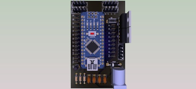
Arduino Nano Breakout Board with full pin breakout screw terminals reset button and reverse polarity protection
Custom ESP32 development board
Custom Arduino Nano board
Bidirectional Visitor Counter
Smart Irrigation System
Line Follower Robotics
What I bring to your project:
Complete KiCad workflow from schematic to layout to Gerbers
2-layer pr multi-layer PCB design optimized for low cost manufacturing
Proper design rules clearances and DRC verification and EMI verification as well before delivery
Clean silkscreen labelling and 3D verification of every board
I take your idea and turn it into a manufacturable board ready to order
Portfolio
Experience
-
Self employed
Self Employed · Freelance
Aug 2025 –
Present
11 mos
United States
PCB Design Projects (KiCad)
Arduino Nano Breakout Board
Custom ESP32 Development Board
Custom Arduino Nano Board
Bidirectional Visitor Counter
Line Follower Robot
Smart Irrigation System
Education
- National University of Technology (NUTECH) BS, Electrical engineering, 3.47 2024 – 2028 (expected) Activities and Societies: I am also involved in electronic project competitions and engineering societies at NUTECH where I get to collaborate with fellow engineers work on real problems and push my skills beyond the classroom as well as that i also play football and basketball too
Other experience
-
University Project — Embedded Systems and PCB Design
Worked on a university level project involving embedded systems and PCB design. Contributed to hardware design schematic creation and board layout as part of a team
projects i work with my seniors team were these
BLDC Motor Driver PCB
IoT Sensor Node with ESP32 and onboard antenna
18650 LiPo Battery Management System (BMS) PCB - Freelance PCB Designer Designing custom Multi-layer PCBs for clients using KiCad from schematic all the way to Gerber files ready for manufacturing. Projects include breakout boards embedded system boards and custom development boards optimized for low cost fabrication at JLCPCB and PCBWay
0 followers, 0 following
Age: 22
Joined: June 5, 2026
Last seen: June 16, 2026
Languages
English Full professional proficiency
Urdu Native or bilingual proficiency
Hindi Full professional proficiency
Punjabi (Eastern) Native or bilingual proficiency
Location
Islamabad, Pakistan