
Jude B.
⭐⭐⭐⭐⭐Embedded Syetems, PCB Design, Firmware Development, IoT, Low Power Design
Global rank:
0
/
139,305
Skill pts: 10
About
Hello, Everyone!
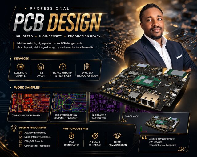
I am an embedded systems engineer, PCB designer, and firmware developer with over 10 years of professional experience. I provide complete, end-to-end solutions for a wide range of electronic device designs, supporting clients from initial concept and schematic design to PCB layout, prototyping, assembly, and full system testing.
I have strong expertise in high-speed PCB design, including PCIe and DDR4 routing, as well as precise impedance matching for reliable performance at high frequencies. I also specialize in RF and antenna design for modern IoT devices, ensuring optimal signal integrity and system efficiency.
In addition, I have deep experience in ultra-low power design, achieving microamp and sub-microamp current consumption for battery-operated and wearable systems.
I specialize in firmware development for LTE-GPS-LoRa-BLE-based embedded systems (nRF52 series), including low-power optimization and high-precision sensor acquisition.
My focus is on delivering robust, production-ready solutions with high reliability and performance.
🔥 Main Skills
👉Embedded Systems
👉Schematic Circuit Design(Low Power consumption Design)
👉Firmware Development(All Microcontrollers-STM32, TMS320, ESP32, FPGA, nRF52, Raspberry PI)
👉PCB Design(High speed signal routing, PCIe, DDR4, 18 multi-Layers Design, RF antenna Design,) using Altium Designer, KiCad, EasyEDA, Fusion 360(No problem in DFM-JLCPCB)
👉IoT with nRF52(BLE), LoRa(for example, SX1262), LTE(SIM card interface), GPS and other variety of sensors
🛠️Tools & Technologies:
👉 nRF5 SDK / nRF Connect SDK
👉SEGGER Embedded Studio + J-Link debugging
👉 C/C++ (bare-metal & RTOS)
👉 BLE GATT, LTE AT commanders, custom wireless protocols
👉SPI / I2C / UART / ADC integration
👉Low-noise measurement systems (nA level)
👉STM32CubeIDE, Cube MX, Keil, CCS, Arduino, ...
👉MQTT, Free RTOS, Zephyr RTOS
🚀 I can support your project from concept to production.
... more »
« less
I am an embedded systems engineer, PCB designer, and firmware developer with over 10 years of professional experience. I provide complete, end-to-end solutions for a wide range of electronic device designs, supporting clients from initial concept and schematic design to PCB layout, prototyping, assembly, and full system testing.
I have strong expertise in high-speed PCB design, including PCIe and DDR4 routing, as well as precise impedance matching for reliable performance at high frequencies. I also specialize in RF and antenna design for modern IoT devices, ensuring optimal signal integrity and system efficiency.
In addition, I have deep experience in ultra-low power design, achieving microamp and sub-microamp current consumption for battery-operated and wearable systems.
I specialize in firmware development for LTE-GPS-LoRa-BLE-based embedded systems (nRF52 series), including low-power optimization and high-precision sensor acquisition.
My focus is on delivering robust, production-ready solutions with high reliability and performance.
🔥 Main Skills
👉Embedded Systems
👉Schematic Circuit Design(Low Power consumption Design)
👉Firmware Development(All Microcontrollers-STM32, TMS320, ESP32, FPGA, nRF52, Raspberry PI)
👉PCB Design(High speed signal routing, PCIe, DDR4, 18 multi-Layers Design, RF antenna Design,) using Altium Designer, KiCad, EasyEDA, Fusion 360(No problem in DFM-JLCPCB)
👉IoT with nRF52(BLE), LoRa(for example, SX1262), LTE(SIM card interface), GPS and other variety of sensors
🛠️Tools & Technologies:
👉 nRF5 SDK / nRF Connect SDK
👉SEGGER Embedded Studio + J-Link debugging
👉 C/C++ (bare-metal & RTOS)
👉 BLE GATT, LTE AT commanders, custom wireless protocols
👉SPI / I2C / UART / ADC integration
👉Low-noise measurement systems (nA level)
👉STM32CubeIDE, Cube MX, Keil, CCS, Arduino, ...
👉MQTT, Free RTOS, Zephyr RTOS
🚀 I can support your project from concept to production.
Portfolio
Service offers
Education
- University of Greenwich Master, Machine Intelligence, null 2022 – 2025 Activities and Societies: null
Other experience
-
Embedded Firmware Development (STM32 | nRF52 | Zephyr RTOS | Low-Power & Real-Time Systems)
These projects highlight my strong expertise in embedded firmware development across multiple platforms, including STM32, nRF52, and RTOS-based systems (Zephyr).
I have hands-on experience working with:
• STM32CubeMX / HAL / LL drivers
• Zephyr RTOS (multi-threading, event-driven architecture)
• Nordic SDK (BLE stack, GATT services, low-power optimization)
• Arduino-based rapid prototyping and sensor integration
Core Strengths:
✔ Real-time system design with task scheduling and event handling
✔ Advanced low-power management (sleep modes, battery monitoring, optimization)
✔ Peripheral integration (ADC, I2C, SPI, UART, GPIO, interrupts)
✔ BLE communication development (custom services, data streaming)
✔ Clean, scalable, and production-ready firmware architecture
What I Deliver:
• Structured and maintainable firmware (C/C++)
• Hardware-aligned driver-level development
• Optimized performance for power, speed, and reliability
• Debug-ready code with clear logging and diagnostics
Summary:
I specialize in building robust, efficient, and production-grade firmware that bridges hardware and software seamlessly.
From low-level drivers to full system behavior, I ensure stable operation in real-world embedded environments. -
FPGA-Based Multi-Channel Professional Audio Processing System
Designed a high-performance audio processing main board based on Xilinx FPGA (XC7A100T), capable of handling multi-channel digital and analog audio signals in real time.
The system integrates multiple professional audio interfaces including AES/EBU, MADI, and Dante network audio, enabling flexible input from various sources. Audio signals are processed through FPGA-based DSP pipelines, including equalization, reclocking, and synchronization using a precision PLL and VCXO clock system to ensure low jitter performance.
- The design features:
• 8-channel DAC output with high-fidelity audio performance
• 2-channel ADC input for analog signal acquisition
• Class-D power amplifier for full-range speaker output
• Dedicated headphone amplifier with protection circuitry
• DDR3 memory interface for high-speed data buffering
• Multi-rail power design including ±15V analog and multiple digital domains
The PCB design required advanced mixed-signal techniques, including:
• High-speed differential routing (LVDS, DDR3)
• Power integrity and thermal considerations for high-current amplifier stages
• Noise isolation between analog and digital domains
• Clock distribution optimization for low-jitter audio performance
This project represents a high-complexity embedded system combining FPGA design, high-speed digital layout, analog audio engineering, and power electronics.
5. High-Speed Embedded System Design (i.MX6 | 14-Layer PCB | 5490 Pins | Power Integrity Optimized)
This project demonstrates my expertise in advanced circuit design and high-speed PCB design for a complex embedded system.
The board is built around a high-performance SoC platform and implemented as a 14-layer PCB with approximately 5,490 pins, requiring precise control of signal integrity, power integrity, and layout optimization.
- Design Highlights:
✔ Complete schematic design for a multi-interface embedded system
✔ Professional 14-layer PCB layout handling high pin-count (5490 pins)
✔ Clean and well-structured power domain separation (analog / digital / high-speed)
✔ Optimized power distribution network (PDN) for stability and low noise
✔ High-speed routing with controlled impedance and proper stack-up design
✔ Complex integration of DDR, Ethernet, USB, PCIe, and other interfaces
- PCB Implementation:
As shown in the layout, the design features:
• Dense high-speed routing with strict length and impedance control
• Clear separation between power and signal domains
• Balanced layer stack-up for EMI/EMC performance
• Efficient component placement for thermal and signal optimization
- Summary:
This project highlights my strength in delivering production-grade hardware design, combining:
• robust schematic architecture
• high-density multi-layer PCB design
• clean power design and signal integrity control -
High Speed Multi-Layers PCB Design
High-Speed Multilayer PCB Design (12-Layer & 8-Layer) for FPGA + DDR4 Systems
This project showcases advanced high-speed PCB design for complex digital systems, including 12-layer and 8-layer stackups developed for FPGA and DDR4 memory integration.
The design focuses on precise high-speed routing between FPGA and DDR4, including strict length matching, controlled impedance routing, and signal integrity optimization to ensure reliable operation at high frequencies.
Key features of this project include:
• High-speed DDR4 routing with tight length matching and timing control
• Controlled impedance design across multilayer stackups
• Optimized layer stackup for signal integrity and power distribution
• Clear separation of analog and digital domains to minimize noise coupling
• EMI-aware layout with proper return path design and ground referencing
• Dense BGA breakout and fan-out routing for high-pin-count FPGA devices
• Careful power integrity design with decoupling strategy and plane management
Special attention was given to minimizing EMI by properly isolating high-speed digital signals from sensitive analog sections, while maintaining continuous return paths and reducing loop areas.
This design reflects a production-ready approach, balancing performance, manufacturability, and reliability for high-speed embedded systems. -
PERS( Personal Emergency Response System)-IoT Wearable Device Development
This device is a medical wearable device for old people and children.
And it is a standalone solution, utilizing LTE connectivity as the primary link. The firmware platform to be used is Zerphy and FreeRTOS. Key features include reliable emergency alerting, secure over-the-air(OTA) updated, and extended battery life, with an option for two-way voice communication. This device doesn’t only include LTE but also GPS, IMU and MCU-STM32 series. -
UMS(Utility Management System) Development
This device is a commercial Intelligent Utility Management System which is a standard “Pre-paid Electricity Meter”. This UMS device consists of 2 parts-Main Control Board and Power Board.
The main control board of this device controls the switching between solar power and grid power on the output board, and measures the output power parameters such as voltage, frequency, current, and power factor, displaying them on the screen.
The main control board was designed using the Raspberry Pi CM5 and provides both LoRa and LTE wireless communication.
Power Board safely switch between these two sources, measure consumption precisely, enforce prepaid credit rules, and supply stable power to main control board for communication and system logic, even during disconnection events.
The maximum supply current of this device is 80 A.
In the PCB design, PCIe, Gigabit Ethernet, USB 3.0, and HDMI differential routing were completed with full impedance matching and length matching, with a deviation controlled within 0.01, ensuring very high signal integrity.
In addition, the power domains between the analog section and the digital section were clearly separated, which effectively solved EMI-related issues.
Stats
0 followers, 0 following
Joined: April 17, 2026
Last seen: July 15, 2026
Area of Expertise
Electrical Engineering
Rapid Prototyping
PCB Design Services
Prototype Design Services
Reverse Engineering
SolidWorks Engineering Services
Prototype Design Engineering
Electronics Design Service
Electrical Schematic Drawing Services
Electrical Instrumentation Services
Electrical Circuit Design Services
Firmware Developers
Software Developers
App Developers
Mobile App Developers
C++ Developers
Android App Developers
Languages
English Native or bilingual proficiency
Location
Harpenden, United Kingdom