I offer PCB design & layout for ESP32, STM32, IoT boards schematic, Gerber, BOM, 3D STEP model



About this service
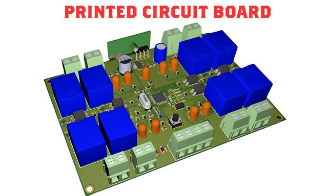
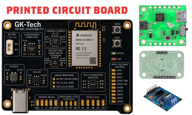
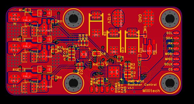
Get a PCB that’s ready to send to the fab, not just a good-looking layout. I take your idea, block diagram or schematic and deliver complete manufacturing files: Gerbers, drill files, BOM, pick-and-place and a 3D STEP model so an enclosure can be designed around your board.
Best for ESP32, STM32, Arduino style and IoT boards: sensor nodes, relay and power boards, USB and serial interfaces, battery-powered devices.
What you get:
• Schematic capture (or cleanup of your existing schematic)
• 2 to 4 layer PCB layout with DRC checks against your fabricator’s rules
• Gerber, drill, BOM and pick-and-place files
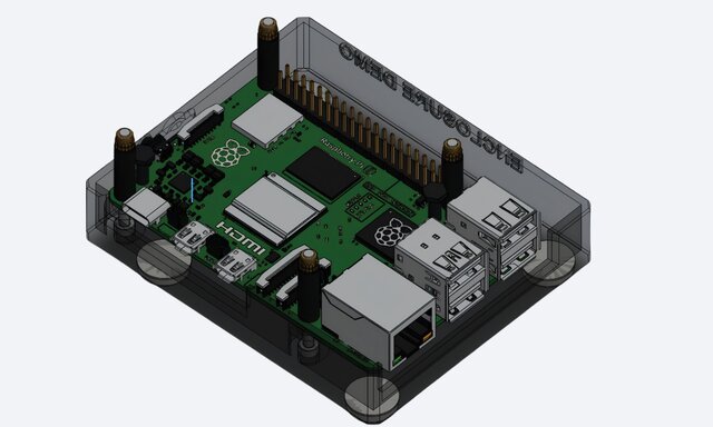
• 3D STEP model for enclosure design
• Source project files on Standard and Advanced
How it works, with your approval at each step:
- You share your requirements and schematic or idea
- I confirm scope, board size and fabricator rules
- Schematic review, then placement preview, then routed layout
- Final files with a handover checklist
I work in [KiCad / Altium / EasyEDA]. Firmware, EMC/CE/FCC certification and assembly are not included unless agreed in a custom quote.
Click Request a service and tell me about your board.
Best for ESP32, STM32, Arduino style and IoT boards: sensor nodes, relay and power boards, USB and serial interfaces, battery-powered devices.
What you get:
• Schematic capture (or cleanup of your existing schematic)
• 2 to 4 layer PCB layout with DRC checks against your fabricator’s rules
• Gerber, drill, BOM and pick-and-place files
• 3D STEP model for enclosure design
• Source project files on Standard and Advanced
How it works, with your approval at each step:
- You share your requirements and schematic or idea
- I confirm scope, board size and fabricator rules
- Schematic review, then placement preview, then routed layout
- Final files with a handover checklist
I work in [KiCad / Altium / EasyEDA]. Firmware, EMC/CE/FCC certification and assembly are not included unless agreed in a custom quote.
Click Request a service and tell me about your board.
Get a PCB that’s ready to send to the fab, not just a good-looking layout. I take your idea, block diagram or schematic and deliver complete manufacturing files: Gerbers, drill files, BOM, pick-and-place and a 3D STEP model so an enclosure can be designed around your board.
Best for ESP32, STM32, Arduino style and IoT boards: sensor nodes, relay and power boards, USB and serial interfaces, battery-powered devices.
What you get:
• Schematic capture (or cleanup of your existing schematic)
• 2 to 4 layer PCB layout with DRC checks against your fabricator’s rules
• Gerber, drill, BOM and pick-and-place files
• 3D STEP model for enclosure design
• Source project files on Standard and Advanced
How it works, with your approval at each step:
- You share your requirements and schematic or idea
- I confirm scope, board size and fabricator rules
- Schematic review, then placement preview, then routed layout
- Final files with a handover checklist
I work in [KiCad / Altium / EasyEDA]. Firmware, EMC/CE/FCC certification and assembly are not included unless agreed in a custom quote.
Click Request a service and tell me about your board.
Best for ESP32, STM32, Arduino style and IoT boards: sensor nodes, relay and power boards, USB and serial interfaces, battery-powered devices.
What you get:
• Schematic capture (or cleanup of your existing schematic)
• 2 to 4 layer PCB layout with DRC checks against your fabricator’s rules
• Gerber, drill, BOM and pick-and-place files
• 3D STEP model for enclosure design
• Source project files on Standard and Advanced
How it works, with your approval at each step:
- You share your requirements and schematic or idea
- I confirm scope, board size and fabricator rules
- Schematic review, then placement preview, then routed layout
- Final files with a handover checklist
I work in [KiCad / Altium / EasyEDA]. Firmware, EMC/CE/FCC certification and assembly are not included unless agreed in a custom quote.
Click Request a service and tell me about your board.
Get a PCB that’s ready to send to the fab, not just a good-looking layout. I take your idea, block diagram or schematic and deliver complete manufacturing files: Gerbers, drill files, BOM, pick-and-place and a 3D STEP model so an enclosure can be designed around your board.
Best for ESP32, STM32, Arduino style and IoT boards: sensor nodes, relay and power boards, USB and serial interfaces, batter... read more
Best for ESP32, STM32, Arduino style and IoT boards: sensor nodes, relay and power boards, USB and serial interfaces, batter... read more
Get a PCB that’s ready to send to the fab, not just a good-looking layout. I take your idea, block diagram or schematic and deliver complete manufacturing files: Gerbers, drill files, BOM, pick-and-place and a 3D STEP model so an enclosure can be designed around your board.
Best for ESP32, STM32, Arduino style and IoT boards: sensor nodes, relay and power boards, USB and serial interfaces, battery-powered devices.
What you get:
• Schematic capture (or cleanup of your existing schematic)
• 2 to 4 layer PCB layout with DRC checks against your fabricator’s rules
• Gerber, drill, BOM and pick-and-place files
• 3D STEP model for enclosure design
• Source project files on Standard and Advanced
How it works, with your approval at each step:
- You share your requirements and schematic or idea
- I confirm scope, board size and fabricator rules
- Schematic review, then placement preview, then routed layout
- Final files with a handover checklist
I work in [KiCad / Altium / EasyEDA]. Firmware, EMC/CE/FCC certification and assembly are not included unless agreed in a custom quote.
Click Request a service and tell me about your board. read less
Best for ESP32, STM32, Arduino style and IoT boards: sensor nodes, relay and power boards, USB and serial interfaces, battery-powered devices.
What you get:
• Schematic capture (or cleanup of your existing schematic)
• 2 to 4 layer PCB layout with DRC checks against your fabricator’s rules
• Gerber, drill, BOM and pick-and-place files
• 3D STEP model for enclosure design
• Source project files on Standard and Advanced
How it works, with your approval at each step:
- You share your requirements and schematic or idea
- I confirm scope, board size and fabricator rules
- Schematic review, then placement preview, then routed layout
- Final files with a handover checklist
I work in [KiCad / Altium / EasyEDA]. Firmware, EMC/CE/FCC certification and assembly are not included unless agreed in a custom quote.
Click Request a service and tell me about your board. read less
Service offer categories
PCB Design Services
Electronic Prototyping and Design Services
Electronics Design Service
Software & skills
3D Enclosures and PCBs
3D PCB LAYOUT
3D PCB Modeling
Altium Designer
Circuit Schematic Design
EasyEDA
KiCad EDA
PCB Design ALTIUM Designer
PCB Layout
Printed Circuit Board Design
+7 more
This service includes
| Service tiers | Simple $90 | Standard $350 | Advanced $650 |
|---|---|---|---|
| Summary | Basic PCB Layout | Complete PCB Package | Complex Board + Documentation |
| Details | 1 to 2 layers, up to about 40 components, schematic capture from your description or layout from your schematic | Up to 4 layers, up to about 100 components, schematic plus layout, power and ground planes | Up to 6 layers, 100+ components, mixed signal or power sections, Wi-Fi/USB modules |
| Delivery time | 4 days | 7 days | 12 days |
| Number of revisions | 0 | 1 | 2 |
Member since
April 2026
Languages
English,
Spanish,
Italian,
French,
Portuguese
Avg. response time
1 hour
3D CAD Designer | SolidWorks| Fusion 360 | Product Design | 3D Printing Mechatronics Engineering
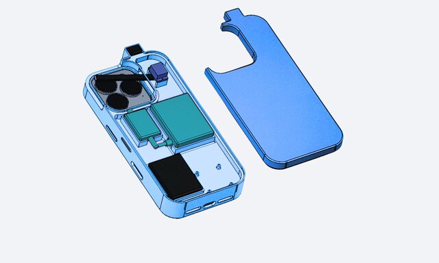
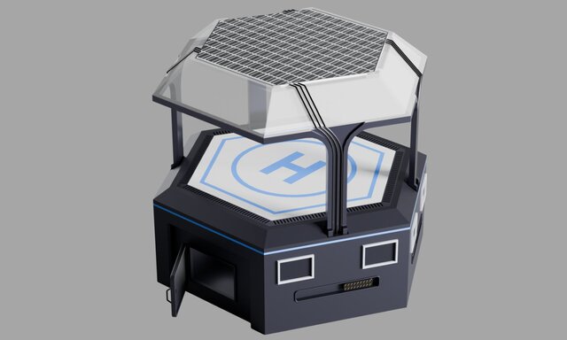
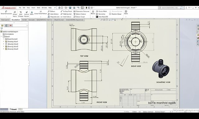
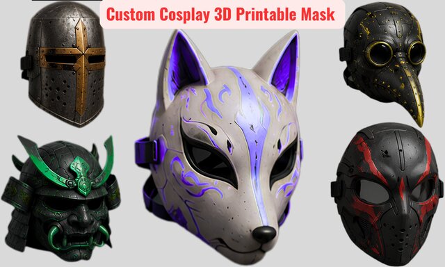
I design 3D CAD models that can actually be built: print-ready parts, product components, enclosures and assemblies in SolidWorks and Fusion 360, delivered as clean STEP, STL, DXF and native files. I also convert 2D drawings and sketches into accurate 3D models and create photorealistic product renders.
I am a Mechatronics Engineering student (B.Eng, Federal University Oye Ekiti) with over 7 year... read more
I am a Mechatronics Engineering student (B.Eng, Federal University Oye Ekiti) with over 7 year... read more
Questions and answers
1.Function: a short description or block diagram of what the board must do.
2.Schematic: your schematic (native file or PDF). If you don’t have one, list the main chips or modules, such as ESP32-S3, STM32F4, sensors, or relays.
3.Size and mounting: board dimensions, mounting-hole positions, and any enclosure or connector placement limits.
4.Power: input source and voltage/current (USB, battery, 12V, etc.).
5.Fabrication: your fabricator, quantity, layer count, thickness, finish, and whether you want assembly.
5.Special constraints: antenna keep-out, high-current traces, or isolation needs. If the board switches mains voltage, say so upfront. It changes spacing and safety requirements, and I may decline or re scope.
6.Existing files: any source project, Gerbers, or reference board you want matched.
7.Deadline.
2.Schematic: your schematic (native file or PDF). If you don’t have one, list the main chips or modules, such as ESP32-S3, STM32F4, sensors, or relays.
3.Size and mounting: board dimensions, mounting-hole positions, and any enclosure or connector placement limits.
4.Power: input source and voltage/current (USB, battery, 12V, etc.).
5.Fabrication: your fabricator, quantity, layer count, thickness, finish, and whether you want assembly.
5.Special constraints: antenna keep-out, high-current traces, or isolation needs. If the board switches mains voltage, say so upfront. It changes spacing and safety requirements, and I may decline or re scope.
6.Existing files: any source project, Gerbers, or reference board you want matched.
7.Deadline.
Both. Send a schematic and I’ll review and lay it out, or send an idea and I’ll draw the schematic for your approval first.
I use [KiCad / Altium / EasyEDA]. Standard and Advanced include the editable project files so you or another engineer can modify the board later.
Tell me whether you’ll use JLCPCB, PCBWay, or another fab, and I’ll set the design rules to match their capabilities.
Simple covers 1 to 2 layers, Standard up to 4, and Advanced up to [6]. Anything beyond that needs a custom quote
I follow standard layout practice and run design-rule checks, but no one can guarantee a board works before a prototype is built and tested. I recommend a small prototype run, and I’ll fix any layout errors in my work during your revisions.
I’ll provide a BOM with part numbers and alternatives where possible. Stock and prices change, so final purchasing is yours.
No. Firmware, CE/FCC/EMC certification, and assembly are not included. I can guide you on ordering assembly from your fabricator, or quote extra work.
Yes, if you send the source project (KiCad, Altium, etc.). Gerber-only boards can’t be edited reliably, so they may need a redraw, which I’ll quote separately.
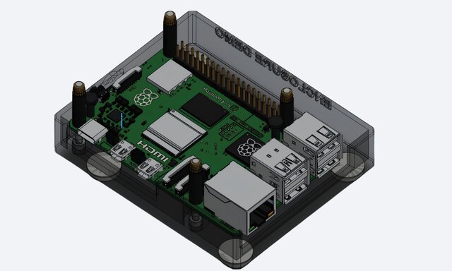
Standard and Advanced include a 3D STEP model of your PCB. A matching 3D printable enclosure is available as an add on or a separate offer.

Cad Crowd Billing Security policy
Service quality is protected by Cad Crowd Billing Security policy.
More from Oluwaseun Olumide A.
More similar services






See related services
- 3D Design services
- 3D Modeling services
- CAD Design services
- 2D & 3D Design services
- CAD Modeling services
- 3D CAD Modeling services
- 2D & 3D Modeling services
- Engineering Design services
- Drafting services
- AutoCAD services
- Mechanical Design services
- 3D Models services
- Design for Manufacturing services
- 2D AutoCAD services
- Product Design services
- Rendering services
- SolidWorks services
- Mechanical Engineering services
- 3D Rendering services
- 3D Solidworks services
- 2D/3D AutoCAD services
- 2D & 3D Modeling Solidworks services
- 3D Printing Design services
- Design Engineer services
- Mechanical Engineer services
- Industrial Design services
- 3D Printing Modeling services
- Product Development services
- Product Design and Development services
- FEA services
- Sheet Metal Design services
- Prototyping services
- 3D Analysis and Design services
- BOM services
- Reverse Engineering services
- Simulation services