I will design professional PCB layouts, schematics and Gerber files


About this service
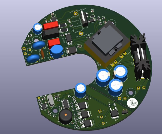
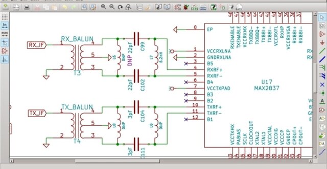
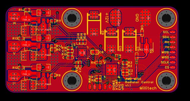
I am a mid-level PCB designer with solid experience in schematic capture, PCB layout, routing, and generating manufacturing files (Gerber, drill, BOM, pick-and-place).
I deliver clean, reliable, and manufacturable PCB designs that work right the first time — optimized for cost, signal integrity, and ease of assembly.
My expertise includes:
- Schematic design and symbol creation
- Multi-layer PCB layout (2 to 6 layers typical)
- Component placement and high-quality routing
- Power and ground planes, decoupling, thermal management
- Design rule checks (DRC), ERC, and manufacturability checks
- Gerber, Excellon drill files, BOM, and assembly drawings
- Basic 3D PCB visualization and step models (if needed)
I mainly work in KiCad (expert level)
Whether you need a simple sensor board, IoT device, power supply, microcontroller board, or a more complex multi-layer design I provide high-quality files ready for fabrication at JLCPCB, PCBWay, or any manufacturer.
I am a mid-level PCB designer with solid experience in schematic capture, PCB layout, routing, and generating manufacturing files (Gerber, drill, BOM, pick-and-place).
I deliver clean, reliable, and manufacturable PCB designs that work right the first time — optimized for cost, signal integrity, and ease of assembly.
My expertise includes:
- Schematic design and symbol creation
- Multi-layer PCB... read more
I deliver clean, reliable, and manufacturable PCB designs that work right the first time — optimized for cost, signal integrity, and ease of assembly.
My expertise includes:
- Schematic design and symbol creation
- Multi-layer PCB... read more
I am a mid-level PCB designer with solid experience in schematic capture, PCB layout, routing, and generating manufacturing files (Gerber, drill, BOM, pick-and-place).
I deliver clean, reliable, and manufacturable PCB designs that work right the first time — optimized for cost, signal integrity, and ease of assembly.
My expertise includes:
- Schematic design and symbol creation
- Multi-layer PCB layout (2 to 6 layers typical)
- Component placement and high-quality routing
- Power and ground planes, decoupling, thermal management
- Design rule checks (DRC), ERC, and manufacturability checks
- Gerber, Excellon drill files, BOM, and assembly drawings
- Basic 3D PCB visualization and step models (if needed)
I mainly work in KiCad (expert level)
Whether you need a simple sensor board, IoT device, power supply, microcontroller board, or a more complex multi-layer design I provide high-quality files ready for fabrication at JLCPCB, PCBWay, or any manufacturer. read less
Service offer categories
PCB Design Services
Electrical Circuit Design Services
Software & skills
3D Enclosures and PCBs
3D modeling & PCB design
Embedded systems PCB
KiCad EDA
+1 more

This service includes
| Service tiers | Simple $120 | Standard $300 | Advanced $700 |
|---|---|---|---|
| Summary | Basic PCB Design | Professional PCB Layout & Schematic | Complex Multi-Layer PCB Design |
| Details | Schematic capture from your description or reference Simple 1 or 2-layer PCB layout (up to 40 components) Basic routing and DRC check Gerber + drill files + BOM | Full schematic design + library creation if needed 2 to 4 layer PCB layout (up to 150 components) Proper grounding, power distribution, and signal routing DRC/ERC + basic signal integrity considerations Complete manufacturing files (Gerber, drill, BOM, pick & place) | Complex schematic and multi-layer PCB (4–6 layers) High component count, mixed-signal, or power electronics Impedance control, differential pairs, thermal vias (basic level) Full design rule verification and manufacturability optimization All production files + 3D STEP model if required |
| Delivery time | 10 days | 15 days | 40 days |
| Number of revisions | 1 | 2 | 4 |
Member since
March 2026
Languages
English
Avg. response time
1 hour
Mechatronics Engineering Student(Solidworks Experience)
Student at University Of Engineering and Technology Lahore.
Just with experience in solidworks 3D modeling.
Have done different Uni-based projects.
I can say that i am not a pro person in this field , buti know i am the person who can make the product pro by giving tie to it.
Just with experience in solidworks 3D modeling.
Have done different Uni-based projects.
I can say that i am not a pro person in this field , buti know i am the person who can make the product pro by giving tie to it.

Cad Crowd Billing Security policy
Service quality is protected by Cad Crowd Billing Security policy.
More from Muhammad J.
More similar services
See related services
- 3D Design services
- 3D Modeling services
- CAD Design services
- 2D & 3D Design services
- 2D & 3D Modeling services
- CAD Modeling services
- Engineering Design services
- Drafting services
- AutoCAD services
- 3D Models services
- Mechanical Design services
- Product Design services
- Rendering services
- 2D AutoCAD services
- CAD Drafting services
- 3D Rendering services
- SolidWorks services
- 3D Solidworks services
- Mechanical Engineering services
- 2D/3D AutoCAD services
- 2D & 3D Modeling Solidworks services
- Industrial Design services
- Mechanical Engineer services
- Design Engineer services
- FEA services
- Product Development services
- Prototyping services
- BOM services
- Simulation services
- Reverse Engineering services
- Electrical Design services
- 3ds Max services
- Blender services
- Autodesk Inventor services
- CAM services
- Electrical Engineering services