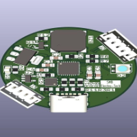
I am an Electronics Engineering undergraduate specializing in PCB design, embedded systems, and hardware development. I design reliable, manufacturable PCBs using KiCad, Altium and...
I am Ahmed Nawaz and Experienced PCB Design Engineer with experience of delivering high-quality and reliable printed circuit board layouts. Proficient in leading industry tools: Al...
Professional Electronic Engineer, and Pcb designer
Abuja,
Nigeria
I’m a highly skilled PCB Designer & Electronic Engineer with years of experience in circuit design, embedded systems, and firmware development. I turn your concepts into production...
I design manufacturable, production-ready PCBs with a focus on power electronics — particularly DC-DC converter layouts, where getting the copper pours, thermal relief, and switchi...
PCB Layout & Engineering | High-Speed, RF, & DFM Optimization Partner - From Your Design to Producti
Milano,
Italy
I offer a complete PCB design service, managed by a team of experienced engineers. I take care of all the critical stages to ensure that your design is not only functional, but als...
I am an Electronics and PCB Design Engineer with hands-on experience in schematic development, PCB layout, circuit simulation, embedded hardware, mixed-signal electronics, and RTL...
I am an electrical and embedded systems engineer specializing in high-reliability hardware for electric vehicles and complex power electronics. Currently engineering powertrains an...
Hi! I am an Electrical and Electronics Engineer specializing in schematic design and PCB layout.
I help clients turn their ideas, circuit diagrams, or prototypes into professiona...
I design medical-grade PCBs for EEG, biosensor and wearable devices - from blank schematic to a validated, manufacturable board.
Most of my work sits where sub-microvolt analog me...
PCB Design Engineer | Cadence Allegro X | PADS Layout
Delhi,
India
I am a PCB Layout Designer with hands-on experience in PCB design and layout development using **Cadence Allegro X PCB Editor and Siemens PADS Layout**.
My expertise includes comp...
3D modeling & PCB designCadence AllegroCadence Allegro PCB DesignerCircuit Design26
more