I will create a PCB design for your startup with Altium and KiCad


About this service
I provide professional Printed Circuit Board (PCB) design services tailored to meet the requirements of electronic products, prototypes, and high-performance systems. My workflow ensures reliability, manufacturability, and compliance with industry standards.
What I Offer
• Schematic Design & Review
Translating your circuit concept into a clean, organized, and error-free schematic with proper component selection and validation.
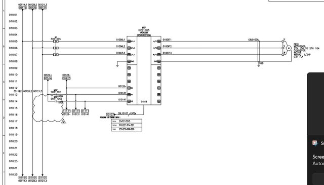
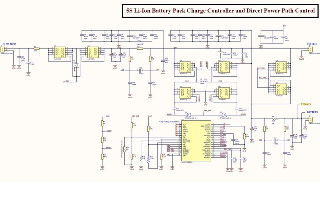
• Professional PCB Layout
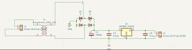
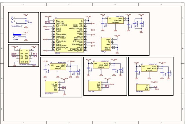
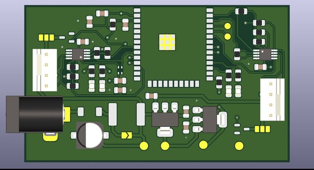
Multi-layer routing with attention to signal integrity, thermal management, impedance control, and optimized component placement.
• High-Speed & RF PCB Design
Specialized layout experience for high-frequency, RF, and antenna-based designs with controlled impedance traces and proper grounding techniques.
• DFM/DFT Optimization
Ensuring your PCB is fully manufacturable and test-friendly according to your preferred PCB manufacturer’s guidelines.
• Documentation & Manufacturing Files
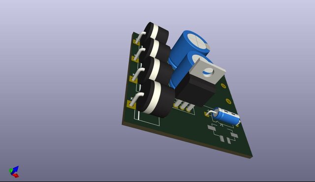
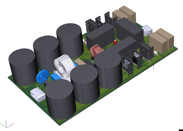
Providing complete deliverables including Gerber files, BOM, pick-and-place files, assembly drawings, stack-up, and 3D PCB model.
Key Capabilities
• 1–8 layer boards
• Mixed-signal designs (Analog + Digital)
• High-power and high-current routing
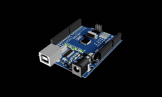
• Sensor-based systems (IoT, ESP32, STM32, Arduino…)
• RF and antenna-integrated PCB
• EMI/EMC-aware routing
• Rigid, flex, and rigid-flex PCBs
Tools Used
• Altium Designer
• KiCad
• Eagle
• Proteus
• CST / HFSS for RF-related designs
Why Work With Me?
• Engineering background in Electroni... read more
What I Offer
• Schematic Design & Review
Translating your circuit concept into a clean, organized, and error-free schematic with proper component selection and validation.
• Professional PCB Layout
Multi-layer routing with attention to signal integrity, thermal management, impedance control, and optimized component placement.
• High-Speed & RF PCB Design
Specialized layout experience for high-frequency, RF, and antenna-based designs with controlled impedance traces and proper grounding techniques.
• DFM/DFT Optimization
Ensuring your PCB is fully manufacturable and test-friendly according to your preferred PCB manufacturer’s guidelines.
• Documentation & Manufacturing Files
Providing complete deliverables including Gerber files, BOM, pick-and-place files, assembly drawings, stack-up, and 3D PCB model.
Key Capabilities
• 1–8 layer boards
• Mixed-signal designs (Analog + Digital)
• High-power and high-current routing
• Sensor-based systems (IoT, ESP32, STM32, Arduino…)
• RF and antenna-integrated PCB
• EMI/EMC-aware routing
• Rigid, flex, and rigid-flex PCBs
Tools Used
• Altium Designer
• KiCad
• Eagle
• Proteus
• CST / HFSS for RF-related designs
Why Work With Me?
• Engineering background in Electroni... read more
I provide professional Printed Circuit Board (PCB) design services tailored to meet the requirements of electronic products, prototypes, and high-performance systems. My workflow ensures reliability, manufacturability, and compliance with industry standards.
What I Offer
• Schematic Design & Review
Translating your circuit concept into a clean, organized, and error-free schematic with proper component selection and validation.
• Professional PCB Layout
Multi-layer routing with attention to signal integrity, thermal management, impedance control, and optimized component placement.
• High-Speed & RF PCB Design
Specialized layout experience for high-frequency, RF, and antenna-based designs with controlled impedance traces and proper grounding techniques.
• DFM/DFT Optimization
Ensuring your PCB is fully manufacturable and test-friendly according to your preferred PCB manufacturer’s guidelines.
• Documentation & Manufacturing Files
Providing complete deliverables including Gerber files, BOM, pick-and-place files, assembly drawings, stack-up, and 3D PCB model.
Key Capabilities
• 1–8 layer boards
• Mixed-signal designs (Analog + Digital)
• High-power and high-current routing
• Sensor-based systems (IoT, ESP32, STM32, Arduino…)
• RF and antenna-integrated PCB
• EMI/EMC-aware routing
• Rigid, flex, and rigid-flex PCBs
Tools Used
• Altium Designer
• KiCad
• Eagle
• Proteus
• CST / HFSS for RF-related designs
Why Work With Me?
• Engineering background in Electronics, Wireless Communications, and Radar systems
• Clean, optimized, and professional layouts
• Fast response and delivery
• Support from concept to production read less
I provide professional Printed Circuit Board (PCB) design services tailored to meet the requirements of electronic products, prototypes, and high-performance systems. My workflow ensures reliability, manufacturability, and compliance with industry standards.
What I Offer
• Schematic Design & Review
Translating your circuit concept into a clean, organized, and error-free schematic with proper com... read more
What I Offer
• Schematic Design & Review
Translating your circuit concept into a clean, organized, and error-free schematic with proper com... read more
I provide professional Printed Circuit Board (PCB) design services tailored to meet the requirements of electronic products, prototypes, and high-performance systems. My workflow ensures reliability, manufacturability, and compliance with industry standards.
What I Offer
• Schematic Design & Review
Translating your circuit concept into a clean, organized, and error-free schematic with proper component selection and validation.
• Professional PCB Layout
Multi-layer routing with attention to signal integrity, thermal management, impedance control, and optimized component placement.
• High-Speed & RF PCB Design
Specialized layout experience for high-frequency, RF, and antenna-based designs with controlled impedance traces and proper grounding techniques.
• DFM/DFT Optimization
Ensuring your PCB is fully manufacturable and test-friendly according to your preferred PCB manufacturer’s guidelines.
• Documentation & Manufacturing Files
Providing complete deliverables including Gerber files, BOM, pick-and-place files, assembly drawings, stack-up, and 3D PCB model.
Key Capabilities
• 1–8 layer boards
• Mixed-signal designs (Analog + Digital)
• High-power and high-current routing
• Sensor-based systems (IoT, ESP32, STM32, Arduino…)
• RF and antenna-integrated PCB
• EMI/EMC-aware routing
• Rigid, flex, and rigid-flex PCBs
Tools Used
• Altium Designer
• KiCad
• Eagle
• Proteus
• CST / HFSS for RF-related designs
Why Work With Me?
• Engineering background in Electronics, Wireless Communications, and Radar systems
• Clean, optimized, and professional layouts
• Fast response and delivery
• Support from concept to production read less
Service offer categories
PCB Design Services
Electronics Design Service
Electrical Circuit Design Services
Software & skills
Circuit Schematic Design
Electronic Hardware Design
KiCAD PCB
KiCad
PCB Design
Printed Circuit Board Design
Proteus
RF PCB design
electronic circuit
+6 more
This service includes
| Service tiers | Simple $20 | Standard $30 | Advanced $50 |
|---|---|---|---|
| Summary | PCB Design for single layer | Double-Layer PCB Design (2-Layer PCB) | Multi-Layer PCB Design (4-Layer / 6-Layer / above |
| Details | Single-Layer PCB Design (1-Layer PCB) Ideal for simple, low-cost, and mass-production designs. Service Includes • Schematic creation or review • Component placement optimized for space and manufacturability • Single-layer routing focusing on: • Clear trace organization • Minimum vias • Easy fabrication • Power distribution optimization • Silkscreen and board outline design • Output package: Gerber files, drill files, BOM, and 3D model | Perfect for moderately complex circuits requiring improved routing and stability. Service Includes • Professional schematic capture • Optimized placement with separation between digital, analog, and power paths • Two-layer routing with: • Power and GND optimization • Short, clean signal paths • Lower noise • Design for manufacturability (DFM) • 3D board visualization and mechanical verification • Complete fabrication package: Gerber, NC Drill, BOM, | For advanced, high-speed, RF, or dense electronics where signal integrity and EMI performance matter. Service Includes • Full schematic design + design review • Layer stack-up planning (controlled impedance, reference planes, material selection) • High-speed routing (DDR, USB, Ethernet, LVDS, SPI @ high frequency) • RF routing & antenna integration (if applicable) • Power integrity (PI) optimization • Thermal analysis planning and copper planes And all services in other services |
| Delivery time | 7 days | 7 days | 15 days |
| Number of revisions | 5 | 5 | 5 |
Member since
November 2025
Languages
Arabic,
English
Avg. response time
1 hour
RF/ Electronic/Mechanic engineer professional with antenna/ PCB design/Mechanical design/3D MODEL
Antenna designer
-Circuit Design
-PCB Designer
-ARDUINO IDE
3D Modelling
AutoCAD
-javascript
-python
-mobile app develpment (android , IOS)
-solidworks
- CST Microwave Studio
-ANSYS HFSS
-Sonar equipment Operation and maintenance
-Radar operator and maintenance maintenance .
-MATLAB , Simulink , GUI
-Multisim, Kicad
-C++C++
-Logo Design
-Adobe Photoshop
-Radar System Engineer and underwater ac... read more

Cad Crowd Billing Security policy
Service quality is protected by Cad Crowd Billing Security policy.
More similar services
From
$100
See related services
- 3D Design services
- 3D Modeling services
- CAD Design services
- 2D & 3D Design services
- 2D & 3D Modeling services
- CAD Modeling services
- Engineering Design services
- AutoCAD services
- Drafting services
- 3D Models services
- Mechanical Design services
- Product Design services
- Rendering services
- 2D AutoCAD services
- Design for Manufacturing services
- CAD Drafting services
- 3D Rendering services
- SolidWorks services
- 3D Solidworks services
- Mechanical Engineering services
- 2D/3D AutoCAD services
- 2D & 3D Modeling Solidworks services
- Mechanical Engineer services
- Design Engineer services
- Product Development services
- FEA services
- Prototyping services
- BOM services
- Reverse Engineering services
- Simulation services
- Electrical Design services
- Autodesk Inventor services
- 3ds Max services
- Blender services
- Electronics Design services
- PCB Design services