I will design your circuit and PCB for JLCPCB manufacturing

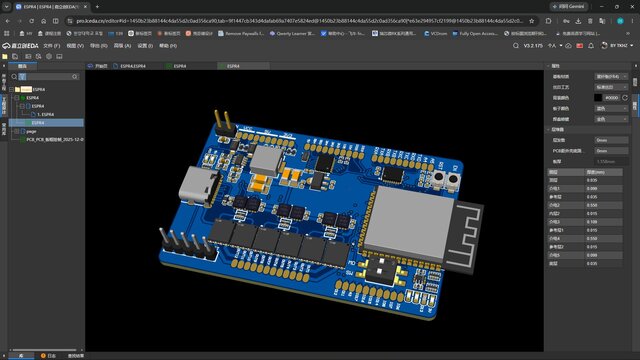
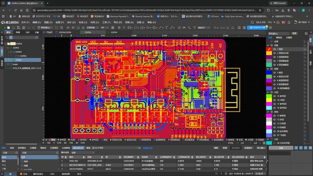
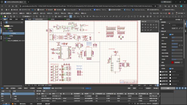


About this service
Practical Circuit & PCB Design - From Design to Manufacturing
I have 8 years of hands-on electronics experience in circuit design, PCB development, embedded hardware, prototyping, debugging, and manufacturing.
What I Can Provide:
- Schematic design and circuit review
- PCB layout up to 8 layers
- Embedded hardware, ESP32/MCU, sensors and peripheral circuits
- Power supply and power management circuits
- Component selection and BOM optimization
- LCSC/JLCPCB component sourcing
- PCB/PCBA optimization for JLCPCB manufacturing
- Gerber, BOM, Pick & Place and other manufacturing files
- EasyEDA source project files
- JLCPCB Manufacturing Advantage
As a Chinese electronics engineer, I have extensive practical experience manufacturing PCBs through JLCPCB and sourcing components through LCSC.
I am familiar with JLCPCB's PCB/PCBA manufacturing process, component system and production requirements.
I also have direct contact with JLCPCB engineers, which can help with quick communication and manufacturing verification when production-related questions arise.
Project Scope
- PCB design up to 8 layers
- Small and clearly defined projects can usually be completed quickly
- High-speed and controlled-impedance PCB designs are available on a project-by-project basis
- For high-speed designs, 4–8 layer stack-ups can be selected according to signal integrity, power distribution, routing and stability requirements
- Complex high-speed projects require sufficient time for proper design an... read more
I have 8 years of hands-on electronics experience in circuit design, PCB development, embedded hardware, prototyping, debugging, and manufacturing.
What I Can Provide:
- Schematic design and circuit review
- PCB layout up to 8 layers
- Embedded hardware, ESP32/MCU, sensors and peripheral circuits
- Power supply and power management circuits
- Component selection and BOM optimization
- LCSC/JLCPCB component sourcing
- PCB/PCBA optimization for JLCPCB manufacturing
- Gerber, BOM, Pick & Place and other manufacturing files
- EasyEDA source project files
- JLCPCB Manufacturing Advantage
As a Chinese electronics engineer, I have extensive practical experience manufacturing PCBs through JLCPCB and sourcing components through LCSC.
I am familiar with JLCPCB's PCB/PCBA manufacturing process, component system and production requirements.
I also have direct contact with JLCPCB engineers, which can help with quick communication and manufacturing verification when production-related questions arise.
Project Scope
- PCB design up to 8 layers
- Small and clearly defined projects can usually be completed quickly
- High-speed and controlled-impedance PCB designs are available on a project-by-project basis
- For high-speed designs, 4–8 layer stack-ups can be selected according to signal integrity, power distribution, routing and stability requirements
- Complex high-speed projects require sufficient time for proper design an... read more
Practical Circuit & PCB Design - From Design to Manufacturing
I have 8 years of hands-on electronics experience in circuit design, PCB development, embedded hardware, prototyping, debugging, and manufacturing.
What I Can Provide:
- Schematic design and circuit review
- PCB layout up to 8 layers
- Embedded hardware, ESP32/MCU, sensors and peripheral circuits
- Power supply and power management circuits
- Component selection and BOM optimization
- LCSC/JLCPCB component sourcing
- PCB/PCBA optimization for JLCPCB manufacturing
- Gerber, BOM, Pick & Place and other manufacturing files
- EasyEDA source project files
- JLCPCB Manufacturing Advantage
As a Chinese electronics engineer, I have extensive practical experience manufacturing PCBs through JLCPCB and sourcing components through LCSC.
I am familiar with JLCPCB's PCB/PCBA manufacturing process, component system and production requirements.
I also have direct contact with JLCPCB engineers, which can help with quick communication and manufacturing verification when production-related questions arise.
Project Scope
- PCB design up to 8 layers
- Small and clearly defined projects can usually be completed quickly
- High-speed and controlled-impedance PCB designs are available on a project-by-project basis
- For high-speed designs, 4–8 layer stack-ups can be selected according to signal integrity, power distribution, routing and stability requirements
- Complex high-speed projects require sufficient time for proper design and verification
- RF/microwave circuit and RF layout design is currently outside my service scope
- I mainly use EasyEDA for PCB design; other commonly used PCB formats can be exported or converted when practical.
- Larger or more complex projects are also welcome when the schedule allows sufficient engineering and verification time
Working Style
I value clear requirements, efficient communication, and practical engineering solutions. My goal is not only to complete the PCB layout, but to provide a design that can be manufactured and assembled reliably.
Please contact me before ordering. I can quickly review your requirements and confirm feasibility, price and delivery time. read less
I have 8 years of hands-on electronics experience in circuit design, PCB development, embedded hardware, prototyping, debugging, and manufacturing.
What I Can Provide:
- Schematic design and circuit review
- PCB layout up to 8 layers
- Embedded hardware, ESP32/MCU, sensors and peripheral circuits
- Power supply and power management circuits
- Component selection and BOM optimization
- LCSC/JLCPCB component sourcing
- PCB/PCBA optimization for JLCPCB manufacturing
- Gerber, BOM, Pick & Place and other manufacturing files
- EasyEDA source project files
- JLCPCB Manufacturing Advantage
As a Chinese electronics engineer, I have extensive practical experience manufacturing PCBs through JLCPCB and sourcing components through LCSC.
I am familiar with JLCPCB's PCB/PCBA manufacturing process, component system and production requirements.
I also have direct contact with JLCPCB engineers, which can help with quick communication and manufacturing verification when production-related questions arise.
Project Scope
- PCB design up to 8 layers
- Small and clearly defined projects can usually be completed quickly
- High-speed and controlled-impedance PCB designs are available on a project-by-project basis
- For high-speed designs, 4–8 layer stack-ups can be selected according to signal integrity, power distribution, routing and stability requirements
- Complex high-speed projects require sufficient time for proper design and verification
- RF/microwave circuit and RF layout design is currently outside my service scope
- I mainly use EasyEDA for PCB design; other commonly used PCB formats can be exported or converted when practical.
- Larger or more complex projects are also welcome when the schedule allows sufficient engineering and verification time
Working Style
I value clear requirements, efficient communication, and practical engineering solutions. My goal is not only to complete the PCB layout, but to provide a design that can be manufactured and assembled reliably.
Please contact me before ordering. I can quickly review your requirements and confirm feasibility, price and delivery time. read less
Practical Circuit & PCB Design - From Design to Manufacturing
I have 8 years of hands-on electronics experience in circuit design, PCB development, embedded hardware, prototyping, debugging, and manufacturing.
What I Can Provide:
- Schematic design and circuit review
- PCB layout up to 8 layers
- Embedded hardware, ESP32/MCU, sensors and peripheral circuits
- Power supply and power management c... read more
I have 8 years of hands-on electronics experience in circuit design, PCB development, embedded hardware, prototyping, debugging, and manufacturing.
What I Can Provide:
- Schematic design and circuit review
- PCB layout up to 8 layers
- Embedded hardware, ESP32/MCU, sensors and peripheral circuits
- Power supply and power management c... read more
Practical Circuit & PCB Design - From Design to Manufacturing
I have 8 years of hands-on electronics experience in circuit design, PCB development, embedded hardware, prototyping, debugging, and manufacturing.
What I Can Provide:
- Schematic design and circuit review
- PCB layout up to 8 layers
- Embedded hardware, ESP32/MCU, sensors and peripheral circuits
- Power supply and power management circuits
- Component selection and BOM optimization
- LCSC/JLCPCB component sourcing
- PCB/PCBA optimization for JLCPCB manufacturing
- Gerber, BOM, Pick & Place and other manufacturing files
- EasyEDA source project files
- JLCPCB Manufacturing Advantage
As a Chinese electronics engineer, I have extensive practical experience manufacturing PCBs through JLCPCB and sourcing components through LCSC.
I am familiar with JLCPCB's PCB/PCBA manufacturing process, component system and production requirements.
I also have direct contact with JLCPCB engineers, which can help with quick communication and manufacturing verification when production-related questions arise.
Project Scope
- PCB design up to 8 layers
- Small and clearly defined projects can usually be completed quickly
- High-speed and controlled-impedance PCB designs are available on a project-by-project basis
- For high-speed designs, 4–8 layer stack-ups can be selected according to signal integrity, power distribution, routing and stability requirements
- Complex high-speed projects require sufficient time for proper design and verification
- RF/microwave circuit and RF layout design is currently outside my service scope
- I mainly use EasyEDA for PCB design; other commonly used PCB formats can be exported or converted when practical.
- Larger or more complex projects are also welcome when the schedule allows sufficient engineering and verification time
Working Style
I value clear requirements, efficient communication, and practical engineering solutions. My goal is not only to complete the PCB layout, but to provide a design that can be manufactured and assembled reliably.
Please contact me before ordering. I can quickly review your requirements and confirm feasibility, price and delivery time. read less
I have 8 years of hands-on electronics experience in circuit design, PCB development, embedded hardware, prototyping, debugging, and manufacturing.
What I Can Provide:
- Schematic design and circuit review
- PCB layout up to 8 layers
- Embedded hardware, ESP32/MCU, sensors and peripheral circuits
- Power supply and power management circuits
- Component selection and BOM optimization
- LCSC/JLCPCB component sourcing
- PCB/PCBA optimization for JLCPCB manufacturing
- Gerber, BOM, Pick & Place and other manufacturing files
- EasyEDA source project files
- JLCPCB Manufacturing Advantage
As a Chinese electronics engineer, I have extensive practical experience manufacturing PCBs through JLCPCB and sourcing components through LCSC.
I am familiar with JLCPCB's PCB/PCBA manufacturing process, component system and production requirements.
I also have direct contact with JLCPCB engineers, which can help with quick communication and manufacturing verification when production-related questions arise.
Project Scope
- PCB design up to 8 layers
- Small and clearly defined projects can usually be completed quickly
- High-speed and controlled-impedance PCB designs are available on a project-by-project basis
- For high-speed designs, 4–8 layer stack-ups can be selected according to signal integrity, power distribution, routing and stability requirements
- Complex high-speed projects require sufficient time for proper design and verification
- RF/microwave circuit and RF layout design is currently outside my service scope
- I mainly use EasyEDA for PCB design; other commonly used PCB formats can be exported or converted when practical.
- Larger or more complex projects are also welcome when the schedule allows sufficient engineering and verification time
Working Style
I value clear requirements, efficient communication, and practical engineering solutions. My goal is not only to complete the PCB layout, but to provide a design that can be manufactured and assembled reliably.
Please contact me before ordering. I can quickly review your requirements and confirm feasibility, price and delivery time. read less
Service offer categories
PCB Design Services
3D Design Services
3D Modeling
Software & skills
Circuit Schematic Design
Electrical Schematics
Embedded Hardware Design
Embedded Systems Design
Embedded Systems Engineering
IoT Hardware Design
PCB Design
PCB Layout
PCB Layout Design
easyeda pro
+7 more
Member since
August 2026
Languages
Chinese (Simplified),
English,
Korean
Avg. response time
1 hour
PCB Designer | 8 Years of Hands-On Electronics Experience | Up to 6-Layer PCB | Embedded Systems & R
I have approximately 8 years of hands-on experience in electronics and circuit development, and I currently work in a university laboratory in South Korea, conducting research related to robotics.
My main areas of experience include embedded systems, robotic electronics, and PCB design. I have practical experience throughout the complete hardware development process, including circuit planning, co... read more
My main areas of experience include embedded systems, robotic electronics, and PCB design. I have practical experience throughout the complete hardware development process, including circuit planning, co... read more
Questions and answers
I have 8 years of hands-on electronics experience and design PCBs up to 8 layers. I focus on practical, manufacturable and reliable designs.
I frequently work with JLCPCB/LCSC and am familiar with their PCB/PCBA and component sourcing process. I can also contact JLCPCB engineers directly when manufacturing verification is needed.
Yes. High-speed and controlled-impedance designs are accepted after project evaluation. RF/microwave designs are currently excluded.
EasyEDA source files, Gerber, BOM, Pick & Place, and other manufacturing files can be provided. Other PCB formats may also be exported or converted when practical.
Small, clearly defined projects can usually be completed quickly. Complex or high-speed projects require additional design and verification time.
As an engineer who values peace and responsible technology, I do not accept weapon-related projects, including weaponized drones or low-cost aerial platforms with a significant potential for military or harmful use.
Before accepting any project, I consider its intended application and potential for weaponization. If I believe there is a substantial risk that the design may be used as a weapon or contribute to armed conflict, I will decline the project.
Before accepting any project, I consider its intended application and potential for weaponization. If I believe there is a substantial risk that the design may be used as a weapon or contribute to armed conflict, I will decline the project.

Cad Crowd Billing Security policy
Service quality is protected by Cad Crowd Billing Security policy.
More similar services





See related services
- 3D Design services
- 3D Modeling services
- CAD Design services
- 3D CAD Design services
- 2D & 3D Design services
- CAD Modeling services
- 2D & 3D Modeling services
- 3D CAD Modeling services
- Engineering Design services
- AutoCAD services
- Drafting services
- 3D Models services
- Mechanical Design services
- Design for Manufacturing services
- 2D Drawing services
- 2D Drafting services
- 2D AutoCAD services
- Product Design services
- CAD Drafting services
- Rendering services
- SolidWorks services
- 3D Rendering services
- Architectural Design services
- Mechanical Engineering services
- 3D Solidworks services
- 2D/3D AutoCAD services
- Assembly Design services
- 2D & 3D Modeling Solidworks services
- Design Engineer services
- Industrial Design services
- Mechanical Engineer services
- Interior Design services
- AutoCAD Mechanical services
- Product Development services
- FEA services
- Sheet Metal Design services