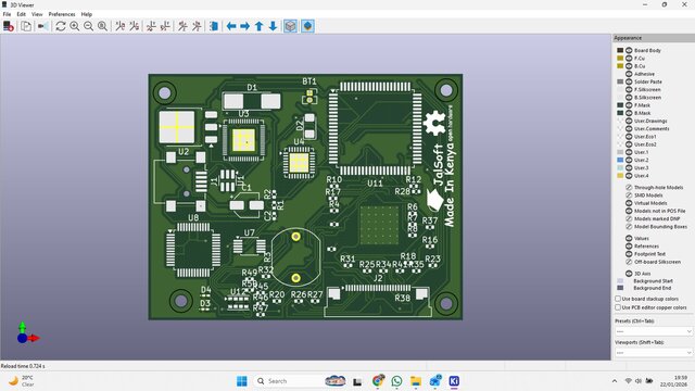
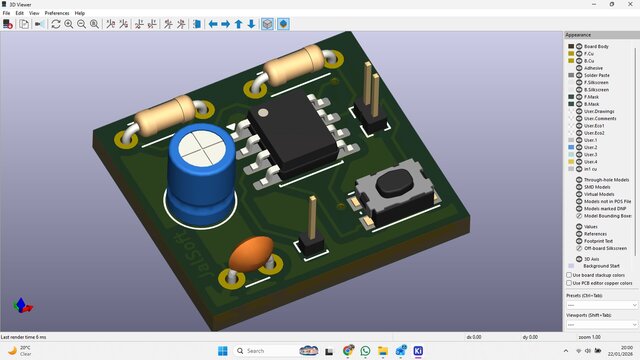


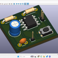
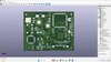
PCB KiCAD design
• Six-layer PCB stack-up configured with dedicated power and ground planes for controlled impedance and low noise coupling.
• Custom 3D component library modeled with exact mechanical dimensions matching manufacturer package specifications.
• Footprint-to-model alignment validated for pad pitch, body outline, and lead geometry accuracy.
• Differential and high-speed traces routed with length matching and return-path continuity considerations.
• Via placement optimized for signal integrity, thermal dissipation, and ground stitching.
• Copper pours and plane segmentation implemented to minimize EMI and maintain stable reference planes.
• Silkscreen, solder mask, and courtyard clearances verified against fabrication tolerances.
• Component placement optimized for signal flow, reduced loop area, and assembly accessibility.
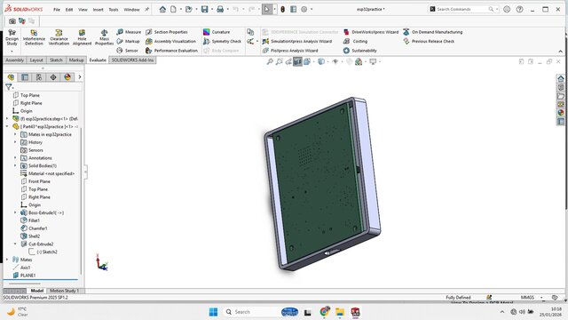
• STEP-compatible 3D models integrated for ECAD–MCAD interoperability and enclosure validation.
• Final layout validated using DRC/ERC checks to ensure manufacturability and electrical reliability.