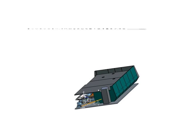


IoT Sensor Enclosure – 3D CAD, Enclosure & PCB Integration Design

PROBLEM
The client's IoT sensing board existed as a bare PCB with no housing. It needed a wall-mountable
enclosure that survives installation, gives access to all connectors, and can be 3D printed for
pilot units before injection tooling.
WHAT I DID
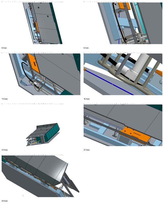
Designed the complete 3D CAD assembly around the existing board outline — mounting boss positions
matched to the PCB fixing holes, cutouts aligned to the USB and sensor locations, cable gland entry
on the base, and a snap-fit lid with screw backup. Wall thickness, draft and fillets were set for
3D printing first and moulding later. Ran interference and tolerance checks across the full
assembly, then iterated two revisions after printing the first unit to correct boss height and
connector clearance.
The PCB itself was designed to fit this mechanical envelope — board outline, mounting holes,
connector placement and cable routing agreed between the housing and the layout, with antenna
keep-out and thermal clearance maintained.
RESULT
A production-ready STEP/STL assembly, 2D fabrication drawings and BOM. The first printed prototype
assembled with the board without modification and the design was handed over ready for tooling
review. Turnaround: 2 weeks concept to printed prototype.
Files delivered: STEP · STL · DXF · BOM · 2D drawings
Published