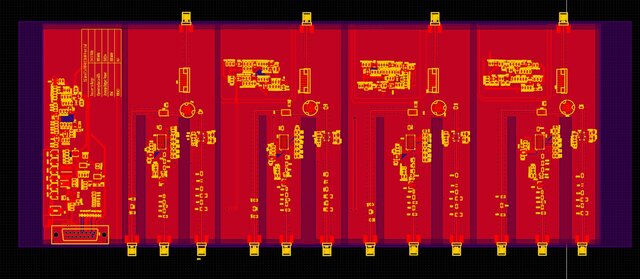
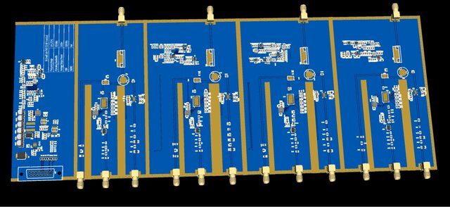
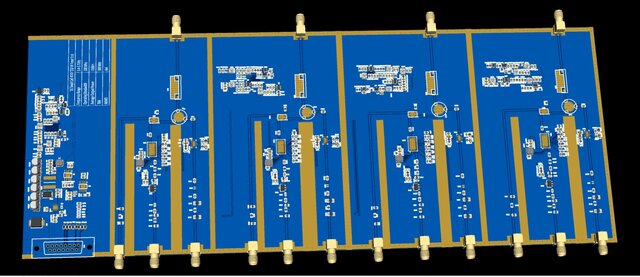
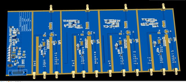


5G RF Front-End 6-Layer Multilayer PCB Design


Designed a 6-layer RF front-end PCB for a 5G telecommunications application while working with ACES – Advanced Communication & Electronic Systems.
The project focused on high-frequency signal integrity and manufacturable multilayer PCB implementation. My work included schematic-to-layout development, controlled-impedance routing, differential pair handling, RF component placement, transmission-line design, impedance matching, via stitching, grounding strategy, and layer-stack considerations for high-frequency performance.
I also prepared the design for manufacturing with DFM/DFT review and complete fabrication documentation.
Published