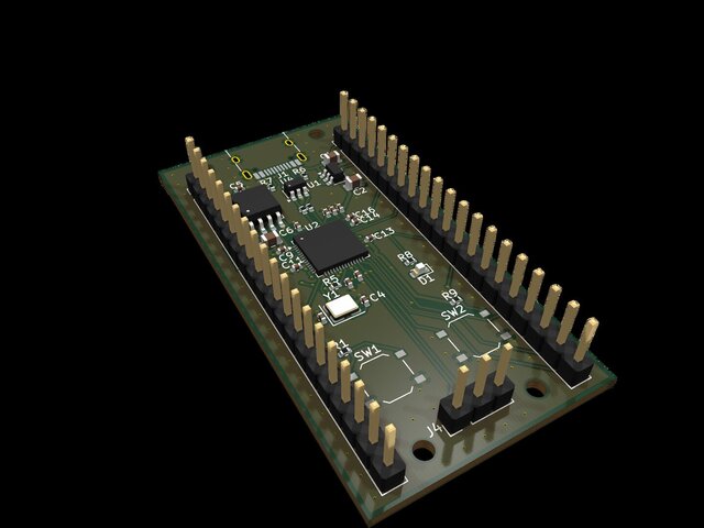
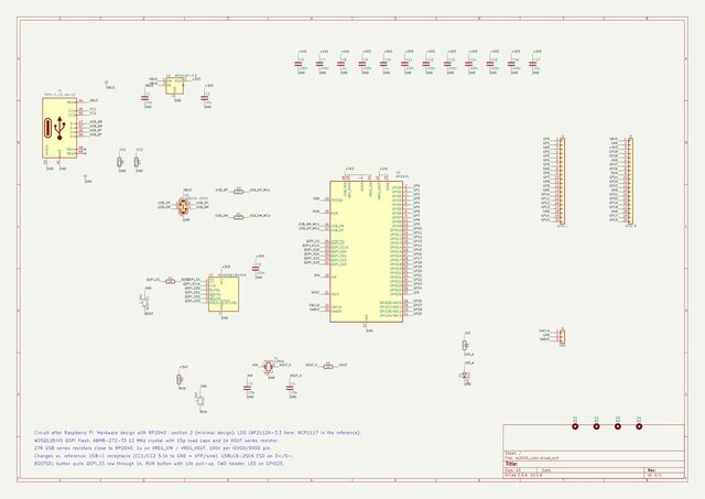
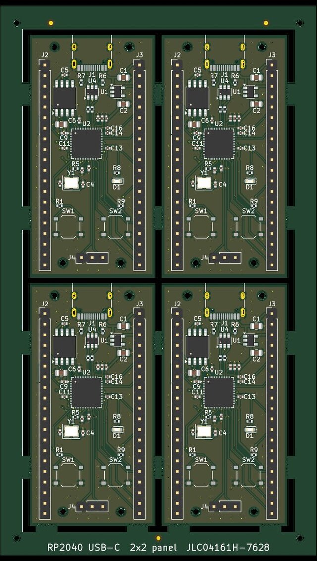
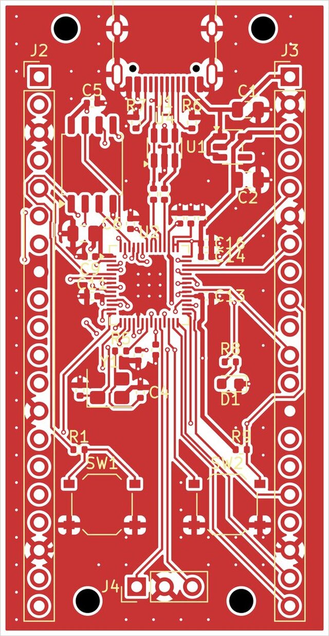


4-layer RP2040 board with USB-C (KiCad, JLCPCB-ready)

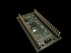
RP2040 development board in KiCad 10, 30 x 58 mm, laid out for the JLCPCB 4-layer stackup JLC04161H-7628.
- USB-C device port wired as a sink, with a 90 ohm USB differential pair (0.27 mm / 0.15 mm, computed and routed by hand through the ESD diode and series resistors)
- 16 MB QSPI flash, 12 MHz crystal, AP2112K 3.3 V LDO, BOOTSEL and RESET buttons
- Fabrication and assembly output: Gerber X2, Excellon drill, BOM with LCSC part numbers, CPL with JLC column names
- 2x2 panel (76 x 132 mm) with rails, tooling holes, fiducials and breakaway tabs kept away from the USB-C edge
- ERC 0 errors, DRC with schematic parity 0 errors, netlist checked pin by pin against the design table, DFM check against JLCPCB's published minimums
The board has not been manufactured yet; all checks are in KiCad and in scripts.