

4-Layer Power Distribution Board: PCB Design Review and DFM

Reviewed, corrected and finalized an existing 4-layer power distribution board for manufacturing. The board accepts a configurable DC/DC converter and distributes multiple voltage rails to a downstream connector, with on/off control logic and status indication. My scope covered full electrical verification, design-for-manufacturing (DFM) correction, component sourcing and production file preparation. It was not a ground-up design, but it needed real design-level engineering judgment to reach a manufacturable state.
The challenge: the supplied design had never been through a full manufacturability check. The first review showed 263 DRC violations and 17 ERC errors, plus several issues that automated checks did not catch at all.
What I found and fixed:
- Stackup: it was left at the CAD tool's generic defaults, giving about 4.67 mm total thickness, almost three times standard. I corrected it to a standard 4-layer 1.6 mm profile with 1 oz copper on all layers for the high-current paths.
- Solder mask: selected high-current traces were meant to be reinforced with solder after fabrication, but default mask tenting would have covered them. I opened the mask over those segments so the rework step is possible.
- Current and creepage: I checked trace widths against the expected load current (IPC-2221) and found an undersized input trace. I verified high-voltage clearances against IPC-2221 tables and enforced them with a custom design rule, with zero violations.
- Component obsolescence: I identified an obsolete LED and an automotive-grade IC that were not available from standard stock, sourced and validated in-stock substitutes, and recalculated the dependent resistor values from the new datasheets.
- Footprint fallout: swapping one IC for an available package changed its pin layout and broke several connections. I rerouted the affected traces and re-verified with DRC.
- Schematic sync bug: I caught a reference designator collision between two unrelated parts that would have confused the assembly file.
Result: DRC violations 263 to 0 errors, ERC errors 17 to 0, board thickness 4.67 mm to 1.6 mm, and two unflagged unavailable parts identified and substituted.
Deliverables: final KiCad project, Gerber and drill files, component placement (CPL) file, BOM with verified part numbers, ERC/DRC resolution report and design notes documenting every engineering decision.
Key takeaway: CAD tool defaults are not the same as a manufacturer's specifications. Stackup, solder mask behaviour and footprint compatibility all need explicit verification, not assumption.
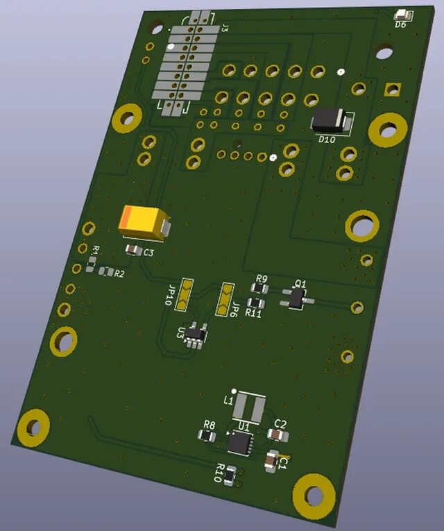
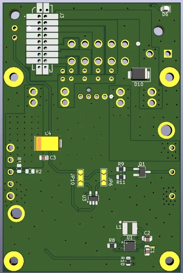
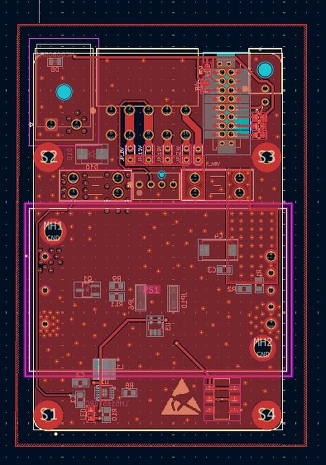
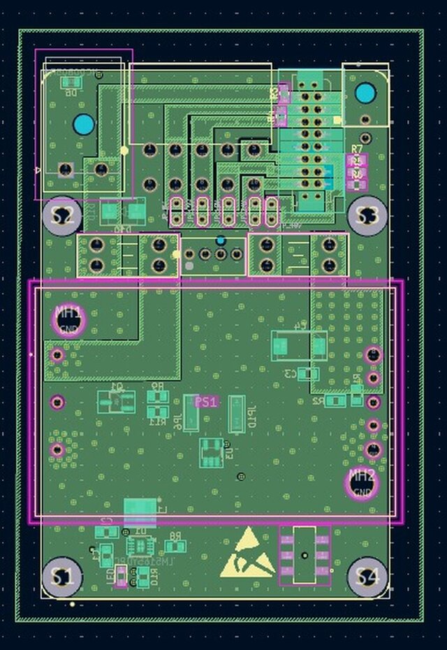
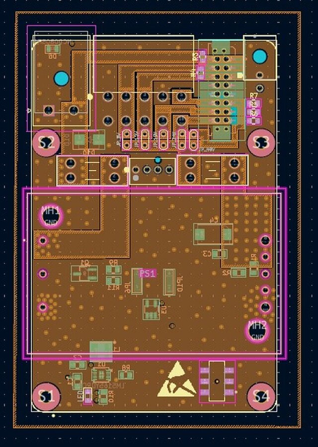
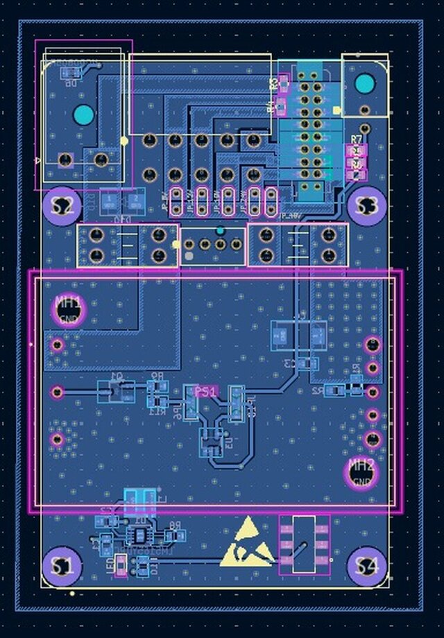
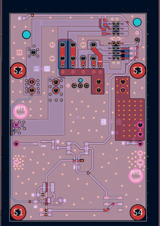
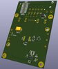
Images show the 3D views and all four copper layers.